Sign In
Upload
Manuals
Brands
NEC Manuals
Microcontrollers
mPD703204Y
NEC mPD703204Y Manuals
Manuals and User Guides for NEC mPD703204Y. We have
1
NEC mPD703204Y manual available for free PDF download: Manual
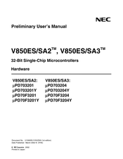
NEC mPD703204Y Manual (518 pages)
32-Bit Single-Chip Microcontrollers
Brand:
NEC
| Category:
Microcontrollers
| Size: 3.22 MB
Table of Contents
Table of Contents
8
Chapter 1 Introduction
23
Overview
23
Features
24
Application Fields
25
Ordering Information
26
V850Es/Sa2
26
V850Es/Sa3
26
Pin Configuration (Top View)
27
Function Block Configuration
31
Internal Block Diagram
31
Internal Units
33
Chapter 2 Pin Functions
36
Pin Function List
36
Pin Status
43
Description of Pin Functions
44
Types of Pin I/O Circuits, I/O Buffer Power Supplies, and Connection of Unused Pins
56
Chapter 3 Cpu Function
60
Features
60
CPU Register Set
61
Program Register Set
62
System Register Set
63
Operation Modes
69
Address Space
70
CPU Address Space
70
Image
71
Wrap-Around of CPU Address Space
72
Memory Map
73
Areas
75
Recommended Use of Address Space
79
Peripheral I/O Registers
81
Special Registers
89
Notes
92
Chapter 4 Port Functions
93
Features
93
V850Es/Sa2
93
V850Es/Sa3
93
Basic Configuration of Port
94
V850Es/Sa2
94
V850Es/Sa3
95
Port Configuration
96
Port 0
97
Port 2
104
Port 3
111
Port 4
118
Port 7
128
Port 8
130
Port 9
132
Port CD
147
Port CM
150
Port CS
156
Port CT
161
Port DH
166
Port DL
170
Operation of Port Function
180
Writing Data to I/O Port
180
Reading Data from I/O Port
180
Operation with I/O Port
180
Chapter 5 Bus Control Function
181
Features
181
Bus Control Pins
181
Pin Status When Internal ROM, Internal RAM, or Peripheral I/O Is Accessed
182
Pin Status in each Operation Mode
182
Memory Block Function
183
Chip Select Control Function
184
External Bus Interface Mode Control Function
184
Bus Access
185
Number of Clocks for Access
185
Bus Size Setting Function
185
Access by Bus Size
186
Wait Function
192
Programmable Wait Function
192
External Wait Function
193
Relationship between Programmable Wait and External Wait
193
Programmable Address Wait Function
194
Idle State Insertion Function
195
Bus Hold Function
196
Functional Outline
196
Bus Hold Procedure
197
Operation in Power Save Mode
197
Bus Priority
198
Boundary Operation Conditions
198
Program Space
198
Data Space
198
Bus Timing
199
Chapter 6 Clock Generation Function
205
Overview
205
Configuration
206
Control Registers
208
Operation
211
Operation of each Clock
211
Clock Output Function
211
Prescaler 3
212
Control Register
213
Generation of Baud Rate
214
Chapter 7 Timer/Counter Function
215
16-Bit Timer/Event Counters (TM0 and TM1)
215
Features
215
Function Overview
215
Basic Configuration of 16-Bit Timer/Event Counters (TM0 and TM1)
216
Control Registers
221
16-Bit Timer/Event Counter Operation
226
Application Examples (16-Bit Timer/Event Counter)
233
Cautions (16-Bit Timer/Event Counter)
242
8-Bit Timer/Event Counters 2 to 5 (TM2 to TM5)
243
Function Outline
243
Configuration of 8-Bit Timer/Event Counter N
244
Registers Controlling 8-Bit Timer/Event Counters 2 to 5
246
Operation of 8-Bit Timer/Event Counters 2 to 5
250
Operation as Interval Timer (8 Bits)
250
Operation as External Event Counter (8 Bits)
252
Square-Wave Output Operation (8-Bit Resolution)
253
8-Bit PWM Output Operation
255
Operation as Interval Timer (16 Bits)
258
Operation as External Event Counter (16 Bits)
260
Square-Wave Output Operation (16-Bit Resolution)
261
Cautions
262
Chapter 8 Real-Time Counter Function
263
Function
263
Real-Time Counter Control Registers
264
Operation
270
Initializing Counter and Count-Up
270
Rewriting Counter
270
Controlling Interrupt Request Signal Output
271
Notes
271
Chapter 9 Watchdog Timer Functions
273
Functions
273
Configuration
275
Watchdog Timer Control Registers
275
Operation
278
Operation as Watchdog Timer
278
Operation as Interval Timer
279
Oscillation Stabilization Time Selection Function
280
Chapter 10 A/D Converter
281
Function
281
Configuration
283
Control Registers
285
Operation
290
Conversion Operation
290
Conversion Operation (Power Fail Monitoring Function)
290
Chapter 11 D/A Converter
291
Functions
291
Configuration
292
D/A Converter Control Registers
292
Operation
294
Operation in Normal Mode
294
Operation in Real-Time Output Mode
294
Cautions
295
Chapter 12 Serial Interface Function
296
Features
296
Selecting CSI1 or UART0 Mode
297
Selecting CSI0 or I C Mode
298
Asynchronous Serial Interface N (Uartn)
299
Features
299
Configuration
300
Control Registers
302
Interrupt Requests
309
Operation
310
Dedicated Baud Rate Generator N (Brgn)
322
Cautions
329
Clocked Serial Interface N (Csin)
330
Features
330
Configuration
330
Control Registers
332
Operation
338
Output Pins
341
System Configuration Example
342
I C Bus
343
Configuration
346
C Control Registers
348
I C Bus Mode Functions
359
C Bus Definitions and Control Methods
360
C Interrupt Request (INTIIC)
367
Interrupt Request (INTIIC) Generation Timing and Wait Control
385
Address Match Detection Method
386
Error Detection
386
Extension Code
386
Arbitration
387
Wakeup Function
389
Communication Reservation
390
Cautions
393
Communication Operations
394
Timing of Data Communication
396
Chapter 13 Dma Functions (Dma Controller)
403
Features
403
Configuration
404
Control Registers
405
DMA Source Address Registers 0 to 3 (DSA0 to DSA3)
405
DMA Destination Address Registers 0 to 3 (DDA0 to DDA3)
406
DMA Byte Count Registers 0 to 3 (DBC0 to DBC3)
407
DMA Addressing Control Registers 0 to 3 (DADC0 to DADC3)
408
DMA Channel Control Registers 0 to 3 (DCHC0 to DCHC3)
409
DMA Trigger Factor Registers 0 to 3 (DTFR0 to DTFR3)
410
DMA Bus States
412
Types of Bus States
412
DMAC Bus Cycle State Transition
413
Transfer Mode
414
Single Transfer Mode
414
Transfer Types
414
Two-Cycle Transfer
414
Transfer Object
415
Transfer Type and Transfer Object
415
External Bus Cycles During DMA Transfer (Two-Cycle Transfer)
415
DMA Channel Priorities
416
DMA Transfer Start Factors
416
DMA Transfer End
416
DMA Transfer End Interrupt
416
Terminal Count Output Upon DMA Transfer End
416
Precautions
417
Interrupt Factors
417
Chapter 14 Interrupt/Exception Processing Function
418
Features
418
Non-Maskable Interrupts
421
Operation
423
Restore
424
NP Flag
425
Eliminating Noise on NMI Pin
425
Function to Detect Edge of NMI Pin
425
Maskable Interrupts
427
Operation
427
Restore
429
Priorities of Maskable Interrupts
430
Interrupt Control Register (Xxicn)
434
Interrupt Mask Registers 0 to 2 (IMR0 to IMR2)
436
In-Service Priority Register (ISPR)
437
Maskable Interrupt Status Flag
437
Watchdog Timer Mode Register (WDTM)
438
Eliminating Noise on INTP0 to INTP6 Pins
438
Function to Detect Edge of INTP0 to INTP6 Pins
438
Software Exception
441
Operation
441
Restore
442
Exception Status Flag (EP)
443
Exception Trap
444
Illegal Opcode Definition
444
Interrupt Acknowledge Time of CPU
446
Periods in Which Interrupts Are Not Acknowledged by CPU
447
Chapter 15 Standby Function
448
Overview
448
HALT Mode
451
Setting and Operation Status
451
Releasing HALT Mode
451
IDLE Mode
453
Setting and Operation Status
453
Releasing IDLE Mode
453
Software STOP Mode
455
Setting and Operation Status
455
Releasing Software STOP Mode
455
Securing Oscillation Stabilization Time
457
Subclock Operation Mode
458
Setting and Operation Status
458
Releasing Subclock Operation Mode
458
Sub-IDLE Mode
460
Setting and Operation Status
460
Releasing Sub-IDLE Mode
460
Backup Mode
462
Setting and Operation Status
463
Releasing Backup Mode
464
Control Registers
466
Chapter 16 Reset Function
467
Overview
467
Configuration
467
Operation
468
Chapter 17 Rom Correction Function
471
Overview
471
Control Registers
472
Correction Address Registers 0 to 3 (CORAD0 to CORAD3)
472
Correction Control Register (CORCN)
473
ROM Correction Operation and Program Flow
473
Chapter 18 Flash Memory
475
Features
475
Erasure Unit
476
Writing with Flash Programmer
477
Programming Environment
477
Communication Mode
478
Pin Connection
480
FLMD0 Pin
480
Serial Interface Pin
480
RESET Pin
483
Port Pins (Including NMI)
483
Other Signal Pins
483
Power Supply
483
Programming Method
484
Flash Memory Control
484
Flash Memory Programming Mode
485
Selection of Communication Mode
486
Communication Command
486
Chapter 19 Electrical Specifications (Target)
488
Chapter 20 Package Drawings
514
Advertisement
Advertisement
Related Products
NEC mPD703200
NEC mPD703204
NEC mPD703200Y
NEC mPD703201
NEC mPD703201Y
NEC mPD703207
NEC mPD703207Y
NEC mPD703068Y
NEC mPD703129
NEC MPD703030A
NEC Categories
Monitor
Projector
Server
Telephone
Computer Hardware
More NEC Manuals
Login
Sign In
OR
Sign in with Facebook
Sign in with Google
Upload manual
Upload from disk
Upload from URL